
June 2, 2026
Most people still think the semiconductor war is about one thing:
Who can make the smallest transistor.
That framework is already aging.
The real shift now is happening underneath the surface, where the competition increasingly revolves around system architecture, signal organization, packaging efficiency, and data movement rather than transistor geometry alone.
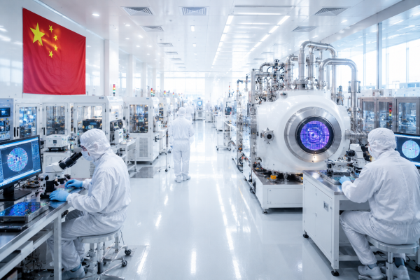
That is why Huawei’s recent “1.4nm-class” announcement matters, even if much of the media coverage misunderstood what was actually being claimed.
The important part was never literal 1.4nm lithography. China still does not possess full frontier EUV capability. Companies like TSMC and Samsung Electronics still dominate advanced fabrication, while ASML remains critical to the entire leading-edge ecosystem. China still faces enormous constraints in tooling, yields, process maturity, and high-end manufacturing consistency.
But Huawei’s announcement was not really a lithography announcement.
It was a systems-engineering announcement disguised as a node announcement.
That distinction changes everything.
The key confusion came from Huawei’s LogicFolding architecture and its broader Tau Scaling framework.
Many people interpreted this almost like a science-fiction flexible processor concept, as if the silicon physically bends inside a folding phone. That is not what Huawei is describing.
The folding happens internally at the logic organization level.
Traditional chip design behaves like a sprawling horizontal city. Signals travel across increasingly dense but still relatively flat layouts. As compute scales upward, communication delays begin consuming more power and more time.
Huawei’s proposed architecture attempts to compress portions of that city vertically into tightly stacked logic districts designed to shorten communication pathways between circuits.
That matters because modern compute increasingly suffers from a movement problem rather than a transistor problem.
Moving information:
- burns power,
- generates heat,
- introduces latency,
- and limits scaling efficiency.
The raw transistor switching event itself is no longer the only bottleneck. In many AI workloads, especially inference-heavy workloads, the larger issue becomes how quickly information moves between memory, compute blocks, and communication pathways.
The industry already knows this.
That is why nearly every major semiconductor company shifted toward:
- chiplets,
- advanced packaging,
- HBM integration,
- unified memory,
- optical interconnects,
- near-memory compute,
- and heterogeneous architectures.
Even NVIDIA’s dominance increasingly comes from ecosystem coordination, memory bandwidth, software integration, and packaging efficiency rather than transistor leadership alone.
Huawei appears to be pushing that same transition further under sanctions pressure.
The company’s Tau framework reportedly focuses on reducing signal propagation delay through shorter communication pathways, vertical logic integration, timing optimization, and folded architectures rather than relying purely on transistor shrinkage.
In simplified form:
Traditional scaling says:
- smaller transistors,
- smaller wires,
- more density.
Huawei’s direction says:
- shorten communication distance,
- optimize pathways,
- stack logic vertically,
- improve effective density architecturally.
That is strategically important because China’s biggest bottleneck remains lithography equipment.
So Huawei appears to be attempting something deeper than simple catch-up.
It is trying to shift the competition from:
“Who has the smallest transistor?”
toward:
“Who organizes compute most efficiently?”
That is a real paradigm-shift attempt.
How important is this actually?
Architecturally, potentially very important.
The semiconductor industry already faces diminishing returns from pure node shrinkage. The cost curves are becoming extreme. Leakage rises, thermal density worsens, yields become more fragile, and capital intensity explodes at advanced nodes.
Everyone in the industry knows classical Moore-style scaling is slowing.
Huawei is attempting to weaponize that slowdown.
If architectural optimization begins mattering more than absolute transistor precision, then China’s relative disadvantages narrow significantly.
That is where the geopolitical implications become serious.
Because China’s strengths are different.
China operates with:
- massive engineering scale,
- vertically integrated manufacturing,
- huge deployment environments,
- state-backed industrial capital,
- aggressive iteration speed,
- and strategic tolerance for lower margins.
Historically, industrial leadership often changes when the battlefield itself changes.
Horse breeders rarely dominate the automobile age.
The danger for Western incumbents is not necessarily that China suddenly surpasses the frontier overnight. The larger danger is that “good enough” compute becomes scalable and cheap enough to reshape the economics of the industry itself.
If China eventually achieves:
- 80–90% practical performance,
- lower production cost,
- massive manufacturing scale,
- integrated domestic ecosystems,
- acceptable yields,
Then, large parts of the world may adopt Chinese computing infrastructure regardless of whether it remains technically “the best.”
That is how industrial dominance often shifts historically.
Not through immediate superiority.
Through scalable sufficiency.
And that is where the real threat begins.
Because once acceptable AI infrastructure becomes dramatically cheaper, pricing power across large portions of the semiconductor stack starts compressing. The same process already appeared in solar manufacturing, telecom infrastructure, EV batteries, and industrial hardware.
China does not necessarily need to dominate the frontier to reshape global economics.
It may only need to become impossible to ignore at scale.
None of this means Huawei magically solved semiconductor physics.
Dense folded architectures create brutal thermal problems. Interlayer synchronization becomes difficult. Power delivery grows more complex. Yield collapse risk rises sharply in stacked systems. Many theoretically brilliant chip concepts fail economically once manufacturing scale becomes necessary.
And there is still no independent evidence proving Huawei currently matches TSMC-class frontier production capability.
That distinction still matters enormously.
But dismissing the broader strategic pattern would also be a mistake.
Because the semiconductor race is visibly evolving from:
“smallest transistor wins”
into:
“best system architecture wins.”
And that shift may ultimately matter more than the headlines themselves.
Huawei’s official timeline for its “1.4nm-class” architecture extends toward roughly 2031. That timeline reveals something important by itself. Even Huawei appears to understand this is not an overnight breakthrough.
It is a long systems transition.
And if that transition succeeds, the real consequence may not be:
“China beat the West at the old game.”
The real consequence may be:
“The old game stopped mattering as much.”